
Apple’s upcoming M5 Pro and M5 Max chips will run cooler and faster than ever before, as a year-old rumor about how Apple Silicon chips are packaged is resurfacing.
Apple is expected to launch the M5 Pro and M5 Max chips as part of the MacBook Pro refresh in early 2026. However, while the higher-end chips are expected to improve performance, the way they are manufactured will have the same impact as the improvements in clock speed and core count.
In a February 3rd Weibo post, serial leaker Fixed Focus Digital added more context to a comment they made a few days earlier on January 31st. At the time, they said the M5’s top chips would use TSMC’s SoIC package, which also lowered operating costs.
In February’s follow-up, the leaker says the benefits of heat dissipation and low drag will be apparent. The change will still be a “2.5D package” with a higher density than “InFo”.
In short, incoming chips will be able to run faster thanks to the package, while also being able to run cooler, minimizing throttling.
While Weibo leakers don’t have a good reputation when it comes to accuracy, Fixed Focus Digital has a rather mixed track record, with some claims proving to be true. However, previous rumors on the subject work in their favor in this case.
Better packaging
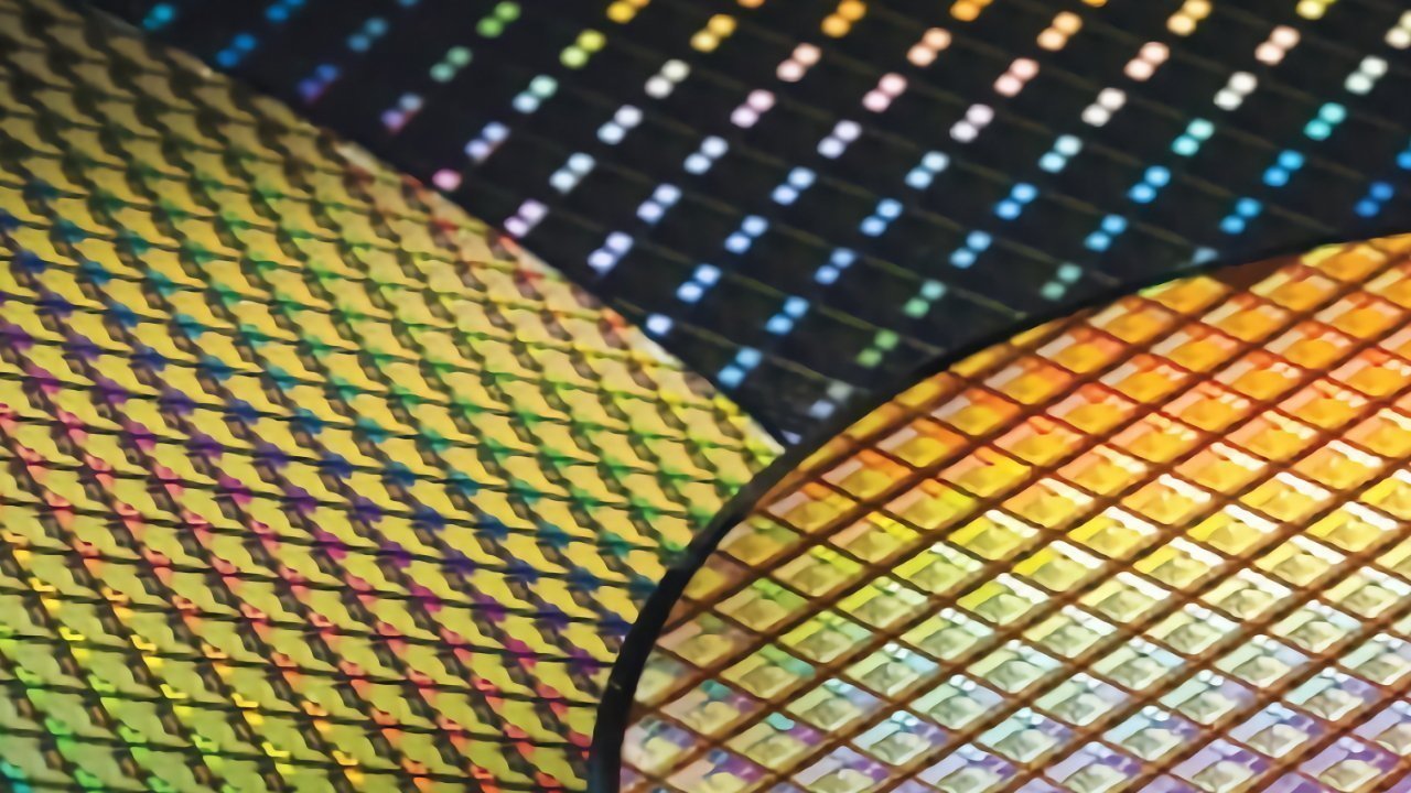
Chip packaging, specifically the process applied to the chip die, is discussed here. It is a crucial element that determines how the chip communicates with other components.
InFo, or Integrated Fan-Out, is the current method used to create very compact chips, such as those used for the iPhone. Its size is certainly advantageous for making thin devices, but it’s a type that’s typically used with single-die rather than multi-die operations.
This is great for efficiency and size, but using one large die can cause thermal issues resulting in throttling.
SoIC, on the other hand, refers to TSMC’s System on Integrated Chips technique. It is a 3D chip stacking process that layers smaller chip parts on top of each other to create a larger chip.
When Fixed Focus Digital refers to this as a “2.5D package”, it means that the smaller matrices are combined side by side on a common inserter. It is a bridging technique between vertically stacked 3D and spread 3D techniques.
This technique offers the benefits of both worlds. There are performance improvements due to tightly coupled dies from 3D packaging, but with the ability to thermally manage the packaging closer to a thin 2D process.
A fundamental change in flexibility
For consumers, the way a chip is packaged can have a much bigger impact on how the chip performs, beyond general performance and thermal improvements.
By using more small forms, there is an opening for Apple to be more flexible with its designs. As previously suggested by Ming-Chi Kuo at the end of 2024, Apple could have separate chiplets for CPU and GPU, so they can be combined in different ways.
Instead of baking the CPU and GPU combination into a single die, TSMC could instead create separate CPU and GPU dies that are assembled in specific configurations in the packaging process.
For consumers, this could mean more choice in terms of CPU and GPU combinations.
For Apple, this will mean a much cheaper way to make chips while maintaining diversity.
The basic cost saving is in the division of the matrix into several parts. Since each CPU and GPU element can be manufactured separately, there should be much higher yields after packaging than if you put them all together on a single die.
This will reduce overall production waste compared to a higher single die failure rate and also potentially reduce the amount of chips.
At a time when memory prices are skyrocketing, this is a much-needed cost-saving measure, especially when demand for chips is extremely high.